Version: 2022-06-04
See also:
-
Java2Vhdl_TranslatorInternals.html - Internals about the implementation
-
../../deploy/Example_J2Vhdl_BlinkingLed-2022-10-21.zip A zip file containing an example and link to the tool base.
-
../../deploy/Example1_BlinkingLed-2022-05-26.zip Old version of zip file.
The next links describe a specific application where this approach is used:
../../../spe/html/SpeA-FPGA/SpeA-JavaFPGA.html This is the description of a FPGA design for SinglePairEthernet PHY layer. Work in progress.
../../../spe/html/SpeA-FPGA/SpeA-FPGA.html The older description based on only VHDL and Aldec-HDL simulation tool using. Comparing both descriptions you can also see advantages in the documentation of the behavior of the FPGA.
This is a preliminary information. The tool Java2Vhdl translator is in progress.
1. Motivation
VHDL was originally created in the 1980th for timing simulations of the behavior of ASICs See https://en.wikipedia.org/wiki/VHDL: In 1983, VHDL was originally developed at the behest of the U.S. Department of Defense in order to document the behavior of the ASICs that supplier companies were including in equipment. … (requested on 2022-05-25)
As a second approach it was later used to determine the content of FPGAs (input for routing).
In the earlier time of FPGA development, till mid of 1990th, usual the timing behavior was evaluated after the routing process, either by timing simulation, or by examination all delays of paths. With some manually settings (placing, special lines manually routed) the routing is repeated till all is met. For that also the VHDL was proper.
From approximately mid of 1990th usage of "timing constraints" become more importance. With timing constraints the router can decide by itself for using routing resources. It means constrains + logical description is sufficient to get a proper FPGA content. The importance of timing simulation is no longer given, at least for most of the FPGA content. Only for clock synchronization approaches or asynchronous parts of logic it is necessary.
The FPGA tool suites support the formulation of timing constraints usual in a special kind. VHDL has not an meaningful contribution for that.
Also the simulation of hardware designs needs often special tools. Test approaches with comprehensive functional tests are a special topic.
For all that reasons another way to formulate hardware design content inclusively timing constraints was searched.
This article offers the idea to formulate hardware design with timing constraints and elaborately possible functional tests, in Java language. The design is oriented to a one clock system as synchronous state machines. The source code which describes that and which is used for the functional tests is then translated to VHDL for the routing process. It means, the full FPGA content can be developed with functional simulation outside of FPGA tool suites. From the FPGA tools so much as necessary can be used, for example only the routine process with timing report (to check whether all is met), or for example also a timing simulation for specific signals outside the functional logic (synchronization with more as one clock or such one). That is all possible of course, but firstly the synchronous part of the design can be planned and tested completely only using a Java development environment (such as Eclipse). This supports also elaborately usage of test possibilities (input signal preparation, evaluation, test control etc.).
2. Why Java and not another language
Java is one of the most known and used programming languages. In opposite to for example C++ Java is a save language. The commonly small programming mistakes by the users do not cause a complicated behavior, they are obviously.
Java knows the final keyword, which is proper to formulate assignments in a unique kind.
That is one of the benefits of the language itself.
The const keyword in C/C++ cannot fulfill the same.
A second benefit is the possibility of formulate annotations, which are recognized also in the run time environment, not only for translation.
See the examples and patterns.
3. Writing hardware logic in Java, principles
There are two different approaches for Fpga content:
-
a) Pure hardware logic
-
b) Using FPGA as platform instead a microcontroller: A microcontroller can react in step times down to ~ 10 µs. 50 µs are often usual. For faster especially controlling algorithm with step times of ~ 1 µs the usage of FPGAs becomes more and more familiar, because the FPGA have enough space, are no more so expensive with much space and the tool suites are more and more proper.
The approach b) is not handled here. They are other tools such as https://hdl.github.io/awesome/items/synthesijer/ or programming FPGA in C++ (known since ~ 2005) which fulfill this approaches.
This work is related to pure hardware logic.
Writing hardware logic in Java requires knowledge about hardware in FPGA. On the first hand should both familiar with the internal structures of logic blocks in your FPGA. Also which such thinks as floorplanner, physical view, timing reports. On the other hand you should familiar with VHDL as hardware description. The VHDL is used as bridge between the Java hardware sources and the place&route tools of the FPGA.
The benefit of writing hardware logic in Java is: Also with a simple tool chain for VHDL and FPGA you can do elaborately tests. The modularity is better supported. Java has a proper software technology (ObjectOrientation, is used also for hardware). Java is often proper known from a large spread of persons. The tool support is well. That are detail advantages.
3.1. Principle of functional simulation of synchronous state machines
Typically, the bulk of the content of an FPGA should be a synchronous design. It means, all input signals are gathered by only one clock, and then furthermore used only clock-synchronous.
All new states are based on the given states with logical relations, which are then adopted as current states with the clock edge.
Qn+1 = fn( Qn)
Whereby the input signals are also part of the Q (means all FlipFlop states). The fn (function) is a logical relation.
To do the same in any sequential programming language, firstly all new states should be calculated from the current states without using the new states itself for calcualtion. That should be done for the whole functionality (not only module per module), because elsewhere new states from already calculated modules may be used by mistake. This new states are the representation of the signal levels on the D inputs of the FlipFlops.
Then the clock edge comes in hardware, that is in software the copy process to declare the new calculated states as current ones. This should be done without logic combinations, only the values are copied.
After that, output values can be calculated from the new current states. Alternatively the output values can also be calculated as the D inputs firstly as new output values, and then copied to the current state of outputs. That are immediately clocked outputs.
For that some step() operations are used in the Java sources, and after them update().
  mdl1.step();
  mdl2.step();
  mdl1.update();
  mdl2.update();
Using Java, some advantages can be uses:
-
The
finalkeyword in Java allows to control settings of variables only one time in a unique kind. Any variable is exactly defined in any control branch. This property of Java can be used to write a clean code.
But the final approach regarding the old (current) states and new states can be only used in the constructors of a class (construction of the instance).
Applicated to the above shown step(); update() approach it means:
-
The
step()create a new instance invoking the constructor and using thefinalapproach for all instance variables. The new instance is not used for otherstep(). -
The
update()copies the new calculated values in the new instances to the current one. In Java all variable to instances are references. Hence it means, the new instances are created withnewin the heap, and referenced with an own reference, and the update copies only the references.
 Type state = new Type();    //initial settings (reset state)
 Type state_d;               //yet null

 ... in a loop:
 state_d = new Type(state, ... more other states );
 ... done firstly for all modules, the step() operations
 state = state_d;            // establish the new states as current
 ... done for all modules, the update() operations.
This is the schema to work in Java for hardware simulation, and also the writing style for translation to VHDL.
3.2. Timing relations
The time to build the logical output from given inputs in the combinatoric logic and lines in the FPGA should be lesser than the time between the clock edges. Then the logical functionality is also the real functionality.
If delays are longer, the behavior is undefined. That is not admissible. It is controlled by the timing constraints.
But not all paths should consider the minimal time between the clock edges. For example you can have a fast clock signal of 200 MHz (5 ns). Some paths should switch in this speed. But not all paths can met the constraint of 5 ns. If the logic is complex, it is a too much requirement. Usage of different clocks for different logic parts is really not a good idea, it requires additional effort for synchronization between the systems. There is a better solution.
Usual the FlipFlops in the Logic Block of a FPGA have a CE input. It is Clock Enable. If this in input is 0, then the signal on the D input has no effect. The FF does not change its state. It means, you can free a FF for switching with a longer period though the clock frequency is high. Only the CE signal should be provided in the required speed for the clock period. The other signals to build the logic need only the CE period respectively the time between two CE='1'.
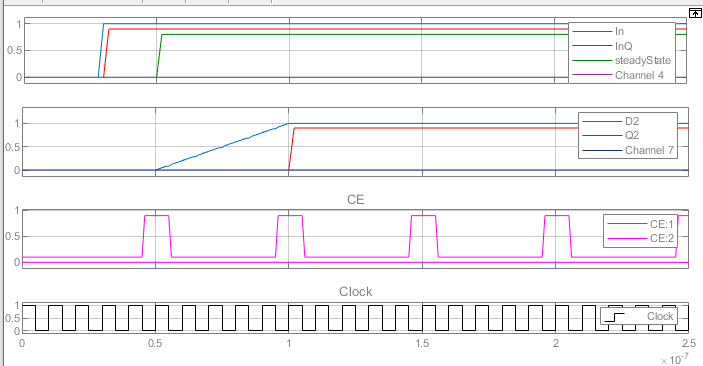
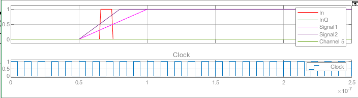
You see the clock in the last track, each rising edge changes the FF state. But the CE signal controls that only each 5th clock edge force switch. In this example the CE is built by a counter which outputs CE exactly after each 5th clock edge. But you see also that CE is delayed. It does not come immediately after the rising clock edge, it does come a little bit later and goes later. The importance is, that CE should be stable on the rising clock, with a minimal necessary setup time. CE can also be delayed, but lesser as one clock period.
In this example the red signal in the first track switches after any rising clock edge, not guarded with CE. But the green signal switches with clock and CE. The next track shows a long delayed signal. It is presented here as ramp, because for simulation Simulink (© Mathworks) is used (not VHDL and a FPGA tool suite). But before the next CE guarded clock edge, the signal arrives its necessary state, and that is sufficient. So the next CE-enabled clock edge gets the state of the delayed signal without failure and produces the next dark green output. This output can also in turn have a delay to its next output, feeding the D input of a FF etc. pp.
In VHDL such behavior can be written in the following form:
PROCESS(CLK, CE) BEGIN
  IF rising_edge(CLK) THEN
    IF CE='1' THEN
      Q2 <= Q1 AND someOtherLogic;
    END IF;
  END IF;
END PROCESS
In VHDL it is determined that nothing should be done if CE is not ='1'.
As ideal case CE is an output of a FlipFlop.
This output is immediately routed to the CE input of all using FF.
For routing a stable clock net with high fan out is used.
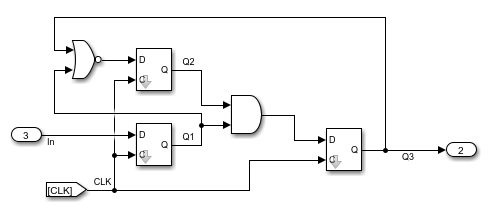
But the router decides by itself how the CE input of the FF in the FPGA are used. See the next slightly changed example:
PROCESS(CLK, CE) BEGIN
  IF rising_edge(CLK) THEN
    IF CE='1' THEN
      IF(steadyState='1') THEN
        Q2 <= Q1 AND someOtherLogic;
      END IF;
    END IF;
  END IF;
END PROCESS
There is another signal as IF condition, here named as steadyState.
Then the routing process can assemble this signal also to build the CE for the FF inputs.
For example if you have a register of 16 or more FF instead the single Q2 and Q1,
it saves a lot of routing resources to do so.
Above you see which may be produced by the router, drawn with ordinary gatter logic. In the real FPGA LUTs (Look Up Tables) are used instead gatter, of course.
How this is related to writing logic in Java
The goal is, determine timeing constrains (see next chapter) for some paths.
In Java you can measure the number of clocks between changing signals,
respectively the number of clocks how long is a given signal in the steady state.
It is very simple. If the signal (variable) is written newly, similar the current time is also stored.
The time is a simple incremented int value (32 bit, sufficient for 1 billion clock steps).
Also a long value may be usable, but seems to be not necessary.
If the signal is used for combinatoric, the current time is compared with the stored time of the input signals. Yet an assertion or warning message can be built if this time difference is lesser than expected.
If you know your own logic, then you know that some signals are set a certain way in respect to the clock because of their functionality. Then you can check in all tests (simulation) whether this programmed and expected behavior is really true - for the test cases. Of course, it depends on the completeness of the tests whether all possible situations are considered. But the logic should not be so complicated that it is non obviously.
Process ( int time, ....) {    //The constructor for new values (see above)
  Fpga.checkTime(time, ref.time, 1);   //assertion with the referenced signal, only 1 clock cycle admissible
  if(ref.ce) {                 //your logic, use a clock enable
    Fpga.checkTime(time, z.time, 10);  //assertion with the own signals, here delay 10 clock cycle admissible
    this.time = time;          //store the time due to the timestamp of possible signal change

    this.signal = z.a && z.b;  //a combinatoric, build a new value, example.
Of course, not every single signal is to be checked, rather the signals are combined into groups with a timestamp in the group. See also chapter Timing constrains for place and route
The expected delay checked with assertions can be used to formulate timing constrains, see following chapter.
3.3. Timing constraints for CE and steadyState
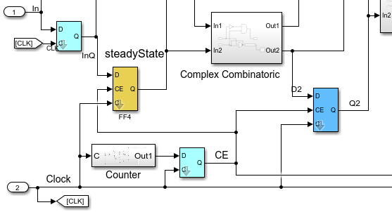
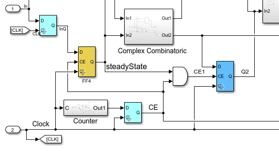
Because the CE is built fastly which each clock edge, it should have a less delay. All FF which should have such an fast delay can be assembled to a FF group, and for that group a constraint can be written (here for Lattice Diamond FPGA tool):
MAXDELAY FROM GROUP "FFfast" 4.5 ns;
But maybe that the steadyState signal does not switch frequently.
It switches only also with the CE signal as shown in the schema above.
Then it can have a longer delay because the fast switching CE signal itself
determines the used CE1 for CE.
It means the FF for steadyState may be a member of the group for CE-driven FF
and can be have a longer delay:
MAXDELAY FROM GROUP "FF_CE" 23.0 ns;
Now the router can use a longer path for the steadyState signal
to build a CE signal for other FF.
The longer delay is possible because this signal does not switch independent,
it switches only with CE itself.
It is not expected that the logic for the CE1 with the longer delayed signal steadyState
or some more other signals produces hazards or glitches because the CE itself is also used
and it has the short delay. It determines the output of the LUT to build the CE1 to 0
so long CE='0'.
3.4. Be careful because of glitches in logic
But you should take care that really one signal with a short path is always member of such an IF construct.
If you write in VHDL
PROCESS(CLK, CE) BEGIN
  IF rising_edge(CLK) THEN
    IF (signal1 XOR signal2)='1' THEN
      Q2 <= Q1 AND someOtherLogic;
    END IF;
  END IF;
END PROCESS
then the router can built a CE to control switching the FF Q2 too.
If the signal1 and signal2 constrain a longer delay as the clock period
then it is possible that a faulty intermediate state can occur
where the signals are detected as different (XOR delivers '1')
though the signals are not different after the delay.
Then the CE can be '1' by mistake during a clock edge.
It means this is a bad formulation in VHDL.
At least one fast signal should be used as AND logic.
Only for info: In Simulink this is produced by the following schema:
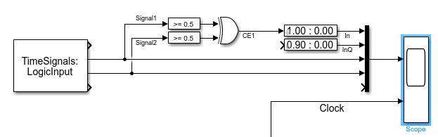
The TimeSignals S-Function-Block is programmed with the given input pattern:
%time:0.000000000: LogicInput.signal1 = 0, LogicInput.signal2 = 0;
%time:0.000000050: LogicInput.signal1 = 0, LogicInput.signal2 = 0;
%time:0.000000100: LogicInput.signal1 => 1.0;
%time:0.000000080: LogicInput.signal2 => 1.0;
See also smlk/…/SmlkTimeSignals.html.
The signals itself are float with ramps, they are converted by the comparison block to boolean,
with that approach a delay can be simulated.
Because the first signal1 reaches the 1-level earlier than the signal2,
temporary the '1' value is built by the XOR. That is a glitch.
If the clock edge comes during the glitch, it is effective and causes a faulty behavior.
Note that the Simulink is not used for FPGA design for this example. It is only used to get simulation results of this hardware. I have used Simulink because it is my familiar simulation environment not only for FPGA, but more for controlling approaches. It should be possible for everybody to use him/here likely tool to get results. The results should be comparable and transferable between the tools.
Automatic check on Java level
The above shown situation can come also from a Java formulated design. It should be possible to check such constructs statically on Java level, yet not clarified. The check should test whether at least one signal is in AND constellation for the whole condition, and this signal should have the less constrain for delay.
3.5. Data types in Java for Fpga design in VHDL
-
VHDL distinguishes between the
BITtype which has two states '1' and '0' (similar as boolean in Java) and adequate also for theSTD_LOGICtype which may have also only the both values '1' and '0' if no more is used on the one hand … -
And on the other hand VHDL knows a boolean type which is strongly used in
IF THENstatements.
There is no automatic conversion between both.
The typical boolean operators AND, OR are valid for all three, the boolean type and also for BIT and STD_LOGIC
but of course with different results. The result follows the inputs, a mix is not possible.
This may be one of the "safety" of the VHDL language, strongly distinguish, but it can be seen also as difficult and confusing.
In Java the situation is clarified with a boolean type which is also strongly and safe:
-
booleanin Java has two states,trueandfalse. -
Better than in C language the
truerepresentation is strongly defined. -
More strongly as in C and C++ language a
ifstatement needs abooleanexpression. All other is faulty.
For the Java representation of a Fpga design with view to VHDL the following is defined:
-
A
booleanvariable represents aSIGNALofBITtype. The valuestrueandfalseare associated to1and0. Negative logic is not supported as language feature. It is a feature of the user’s semantic. -
A
BIT_VECTORis represented by aintorlongvalue (with up to 64 bit). This is better to test in Java as a boolean vector, becauseBIT VECTORis often used as register values, also for shift and compare operations. -
To access one bit of such an vector, there is a special access operation
Fpga.getBit(vector, 7)where7is a bit number. The result of this operation in Java isbooleanwhich is aBITtype. -
Exact the same can be done with a
STD_LOGIC_VECTOR, also represented in Java withintorlong, distinguished only by the annotation@Fpga.BITVECTORor@Fpga.STDVECTOR -
Yet numerical values are not supported, done in the (near) future. The types
shortandintfor 16 and 32 bit bit width without additional annotations should be used for 16- and 32 bit with algorithm (longalso for 64 bit).
3.6. boolean expression and SIGNAL types with view to VHDL
In VHDL, if you have a boolean operation with a BIT or also STD_LOGIC type, you can write:
result <= (a AND NOT b) OR c;
If you do the same for an IF construct you must write:
IF (a='1' AND b='0') OR c='1' THEN
It means the operands should fistly converted to a boolean one. But it is also possible to write:
IF ((a AND NOT b) OR c) ='1' THEN
Here the expression is calculated as bit and then converted to boolean as last action for the IF usage.
But if you have a mix of BIT and STD_LOGIC it is not easy to write.
If b1 .. b3 are BIT types and s1 .. s3 are STD_LOGIC you can write
b3 <= b1 AND b2;
s3 <= s1 AND s3;
But you cannot write a mix of both.
s3 = a1 AND b1;
For that it is necessary to write:
IF(a1='1' AND b1='1') THEN s3 = '1'; ELSE s3 = '0'; END IF;
Now the check is done on compilation level as boolean and the results are set.
For the routing process and the logic in FPGA it is exactly the same if there are no tristate or wired lines or such one,
or better: If the STD_LOGIC signals have in any case only the values '0' and '1'.
It is a property of the language VHDL, which regards that a STD_LOGIC can or may have also other values then '1' and '0'
as possibility. The given line does not give an information about that.
Hence it is a little bit complicated for the code generation.
3.7. Use cases of STD_LOGIC definitions
The STD_LOGIC was introduced in VHDL firstly to support simulation with the values 'U', 'X' etc.
That is unrelated for the Java2Vhdl, because simulation is done in pure VHDL.
But it may be important: If Simulation should be done with VHDL then all SIGNALs should be defined as STD_LOGIC and not as BIT.
Secondly, also important for Java2Vhdl, the Tristate and a wired or or wired and (pullup, pulldown lines) in the FPGA hardware
can only defined with STD_LOGIC.
For that the type
@Fpga.STDLOGIC char mySignal;
supports definition of a data type with the 9 possible states. They are given as characters for the char variable and adequate used for Java simulation.
The other possibility is to define
@Fpga.STDLOGIC boolean mySignal;
In this case this variable is translated to STD_LOGIC, but only the two states '1' and '0' are supported.
4. Modularity, with Object Oriented Approach
Of course, Java is an Object Oriented Language. It is important for ordinary software programming. The important common features for Object Orientation and their relations to hardware description approaches are shown in the following sub chapter.
4.1. Object Orientation approaches and their possibility for VHDL with the Java2Vhdl translator
-
OO: Some related data are combined in a class.
-
VHDL: This is also familiar in VHDL, using a TYPE RECORD and its instances. Secondly the classic modularity with one VHDL file per module fullfils this approach.
-
OO: Some operations are related to the data, the operations which works with the data.
-
VHDL: it is possible to build RECORDs, and PROCESSes, which touches only data of exactly one record instance. It means the RECORD definitions are oriented to the PROCESS definitions. The PROCESS is the operation or "method" related to the data. That is possible, not necessary in VHDL but may be seen as recommended. But other than in Object Oriented writing style the PROCESS can be related only to one RECORD instance and not to the
TYPE RECORD, to the type as in Object Orientation. For the Java2VHDL translator the operation is defined type related of course (because of other reason in the constructor). The translator generates the PROCESSes from that constructor code, but instance related. In the normal software Object Orientation the instance relation is made on run time via the arguments of the method (in particular the instance pointerthis, but also via other referenced instances as arguments). The Java2Vhdl translator resolves this arguments and builds PROCESSes for each instance as result of translation. It can be seen that the realization of the VHDL design is associated with a runtime, while the description in Java is the source for compilation. -
OO: Encapsulation of data. Data can be designated as
privateorprotected. In both cases the data cannot be accessed from any other module, only from the own one ore derived ones in case ofprotected. The package private designation in Java (withoutpublickeyword) is a furthermore possibility similar to thefrienddesignation in C++: Some modules can be associated to access there data one together, but the access is not possible from modules outside of this group.This feature is not firstly for protection, is supports a proper modularity without too much data dependencies.
-
VHDL: In a module in an own VHDL file the data are also encapsulated. But the Java2VHDL translator supports also a flattened style with one VHDL file for some modules and some TYPE RECORD inside. But because of encapsulation of the data in Java, the access to the records are also sorted.
-
OO: aggregated modules: Any module can have references to other modules. In UML (Unified Modelling Language) this references are designated as composition (own sub module), aggregation (hard referenced other module, not changable) and association (changeable). But the access to properties of the other module are organized. Only
publicor package private members can be accessed, see topic above. It is able to clarify whether an access can be done only via access operaions ("getter") or also topublicdata. The data can befinalespecially in Java to forbid writing, changing of the data in another module. This is an essential idea to decrease to much functional dependencies between modules. -
VHDL: In the classic VHDL only the data flow via the Interface data (
ENTITY PORT) is possible. This is not an aggregation concept, it is a dataflow concept.-
But if a
TYPE RECORDis seen as a module, in a flattened design (one file for more modules), then the access to the data to other modules is immediately possible. Last not least, for the deployed design in the FPGA it is the same as using more as one VHDL file with ports. But from the view point of the VHDL source it is maybe more obviosly and more simple to read what`s happen. This is one of the basic idea of the flattened design of the generated VHDL file. -
From view point of the FPGA content description in Java, Aggregations are used, see chapter More possibilities with Java2VHDL: References (aggregations) in Object Orientation kind. Via the aggregations either public data can be accessed immediately, or the better approach is using the interface concept, see Interface technology in Java for VHDL. This is possible via modules in one flattened design.
-
-
OO: There is the possibility to use derived types from an abstract type: The thinking should not be: Have any type, and derive it. The better thinking way is: Have some different types, how to find common properties and their embodiment in an abstract type of all these different types. It means the derivation is the secons approach, the abstraction is the first one. This is done because dealing with common properties (abstraction) is a good idea.
-
OO: Related to Java programming languate, firstly the interface concept is one of the abstraction: Defining of a comman access possibility. The interface is implemented then in any type (class).
-
OO: This feature of Object Orientation is very important for flexibility and testing.
-
A module can be connected to different similar but not necessary equal other types (aggregation in UML).
-
For testing an aggregated module can be replaced by a stub or mock which fullfils the interface for test approaches, to execute module-related (unit) tests.
-
-
VHDL: This is an interesting topic. Also in VHDL a module / unit test may be seen as important. The test can be done in a reduced real desing in an FPGA, and also on software level. Exactly this topic is realized in the Java2Vhdl translator. See chapter Interface technology in Java for VHDL.
4.2. Modularity in classic VHDL
VHDL was developed in a time as Object Orientation was not familiar. And of course, is Object Orientation proper for hardware approaches? Not from the eyes of the 1980th. But from the eyes of hardware test approaches and translation possibilities of the 2020th!
The modularity of VHDL is classic, it is a dataflow approach:
-
Define an interface to a module, this is in the module the ENTITY PORT definition part.
-
This definition part should be repeated on usage as COMPONENT definition with the same content (a disadvantage, In C header files for that are used).
-
On usage secondly in a PORT MAP signals should be connected. The connection of two modules needs extra signals.
 For that the writing and maintain effort is high.
This is especially a problem on refactoring.
The importance of refactoring in modern software technology is some more higher as in the 1980th,
related with the topics agile program development, complexity of solutions.
For that the writing and maintain effort is high.
This is especially a problem on refactoring.
The importance of refactoring in modern software technology is some more higher as in the 1980th,
related with the topics agile program development, complexity of solutions.
The image right side is only an illustration. It shows how two cards with simple plugs can be connected in a simple way. You are responsible to all by yourself, and you can do what ever you want, in this example have a resistor in the line. This is similar as wiring of modules in VHDL. You need an effort, but you can insert your own logic on module plugging level between the modules.
For hardware description in Java a similar approach is possible using an In and Out inner class for the input and output signals.
This is necessary if one module should translated as one module to VHDL.
4.3. More possibilities with Java2VHDL: References (aggregations) in Object Orientation kind
The following example code snippet comes from the example project in the linked zip file on start of this document:
The modules in Java can be implemented in a flattend form in VHDL.
Then each inner class from one Java file (module) is one TYPE RECORD definition in VHDL.
The top level VHDL file or also a module can have some such RECORD TYPE definitions.
Example start of an inner class in a module MyModule.java:
//fpga/exmpl/modules/ClockDivider.java
  /**Inner PROCESS class builds a TYPEDEF RECORD in VHDL and a PROCESS for each instance.
   * Note: Need public because here the interface technology is not used (negative, but simple understandable pattern).
   * Compare with {@link Reset.Q}
   */
  @Fpga.VHDL_PROCESS public static final class Q{

    @Fpga.STDVECTOR(4) final int ct;

    /**This is the variable of the record accessed from outside.
     * Note: Need public because here the interface technology is not used (negative, but simple understandable pattern).
     * Compare with {@link Reset.Q#res}
     */
    public final boolean ce;

    /**Time of the latest set operation of any of the variables. */
    public int time;
Builds the record in VHDL:
TYPE ClockDivider_Q_REC IS RECORD
  ct : STD_LOGIC_VECTOR(3 DOWNTO 0);
  ce : BIT;
END RECORD ClockDivider_Q_REC;
The RECORD is instantiated, here with one instance, but also more as one instances are possible:
SIGNAL ce_Q : ClockDivider_Q_REC;
In VHDL from inside any PROCESS a variable of another module (RECORD instance) can be accessed, because of the flattened form with RECORDS.
ct_Q_PRC: PROCESS ( clk )
BEGIN IF(clk'event AND clK='1') THEN

  IF ce_Q.ce='1' THEN
That is possible because of the flattened property.
This is simple also for the routing process for FPGA tools.
The signal ce in the record instance ce_Q is immediately accessed.
But:
The idea working flattened is bad for the real sources. It means that is not an approach for the Java sources. But instead, the Java sources can work with aggregations. The adequate line in Java for the process of the other module looks like:
//fpga/exmpl/modules/BlinkingLedCt.java
    @Fpga.VHDL_PROCESS Q(int time, Q z, Ref ref, Modules modules) {
      Fpga.checkTime(time, ref.clkDiv.q.time, 1);  // for the ce signal, constraint with 1 clock delay.
if(modules.ct_clkDiv.q.ce) {-
In Java the access is not done immediately to the variable in the other class. Instead a reference
ref.clkDivis used. -
Whereby
refis a module specific instance which holds all references,clkDivis the reference to the other module. -
The name after
ref.clkDivis not related to Vhdl. It is a local name in the module class in Java, not related to the really used instance. -
This is due to modularity. A module should not know which concrete instance of another module is used. This is not to be clarified in the module. It must be clarified in the higher-level programming which uses the modules.
How it is related:
Any module can contain a Ref class with a Ref ref instance, here:
//fpga/exmpl/modules/BlinkingLedCt.java
  private static class Ref {

    /**Common module for save creation of a reset signal. */
    final Reset_ifc reset;

    final BlinkingLedCfg_ifc cfg;

    /**Specific module for clock pre-division. */
    final ClockDivider clkDiv;

    Ref(Reset_ifc reset, BlinkingLedCfg_ifc cfg, ClockDivider clkDiv) {
      this.reset = reset;
      this.cfg = cfg;
      this.clkDiv = clkDiv;
    }
  }

  private Ref ref;
That are aggregations in UML wording (Unified Modeling Language for Object Orientated software technology).
As you see the name of the referenced module clkDiv is a private name, not the name of an existing instance in the parent module.
This is per se unknown, not determined which modules and also which type of modules are used.
The constructor of the Ref have to be called in the constructor of the module, because ref is final:
//fpga/exmpl/modules/BlinkingLedCt.java
  /**Module constructor with public access to instantiate.
   * <br>
   * Note: The arguments should have the exact same name and type as in the {@link Ref#Ref(Reset_ifc, ClockDivider)} inner class.
   *
   * @param reset module provide the reset signal on power on and as input
   * @param clkDiv module provide a clock enable signal: {@link ClockDivider.Q#ce}
   */
  public BlinkingLedCt ( Reset_ifc reset, BlinkingLedCfg_ifc cfg, ClockDivider clkDiv) {
    this.ref = new Ref(reset, cfg, clkDiv);
  }

  /**Non parametrized constructor if the aggregations are not existing yet. Use {@link #init(Reset_ifc, BlinkingLedCfg_ifc, ClockDivider)}
   * for aggregation. */
  public BlinkingLedCt () {}
  /**The init operation should be used instead the parameterized constructor with arguments if there are circular dependencies:
   * The modules should be known each other. Then only one module can be instantiated with the parameterized constructor.
   * The other module can only be instantiated firstly without aggregations, then get the aggregation via this init operation.
   * <br>
   * Note: The arguments should have the exact same name and type as in the {@link Ref#Ref(Reset_ifc, ClockDivider)} inner class.
   * @param reset aggregation to the reset module.
   * @param cfg aggregation to the configuration
   * @param clkDiv aggregation to the clock divider.
   */
  public void init ( Reset_ifc reset, BlinkingLedCfg_ifc cfg, ClockDivider clkDiv) {
    this.ref = new Ref(reset, cfg, clkDiv);
  }
Here it is important that the name of the arguments in the constructor is the same as the name of the aggregation reference
in the Ref class. That is not a problem and also a good style. It is necessary for the translation to VHDL.
Now, in the top level in Java all modules should be instantiated. The Java-toplevel decides which modules are used.
For that there is a Modules inner class:
//fpga/exmpl/modules/BlinkingLedCt.java
  /**The modules which are part of this Fpga for test. */
  public class Modules {

    /**The i/o pins of the top level FPGA should have exact this name ioPins. */
    public BlinkingLed_FpgaInOutput ioPins = new BlinkingLed_FpgaInOutput();

    /**Build a reset signal high active for reset. Initial or also with the reset_Pin.
     * This module is immediately connected to one of the inputFpga pins
     * via specific interface, see constructor argument type.
     */
    public final Reset res = new Reset(this.ioPins.reset_Inpin);

    public final Test_Combinatoric_BlinkingLed vhdl_Combinatoric = new Test_Combinatoric_BlinkingLed();

    public final BlinkingLedCt ct = new BlinkingLedCt(this.res, BlinkingLed_Fpga.this.blinkingLedCfg, this.ce);    //cfg implemented in extra class in this file.

    public final ClockDivider ce = new ClockDivider(this.res, this.ct);

    Modules ( ) {
      //aggregate the module afterwards
      this.ct.init(this.res, BlinkingLed_Fpga.this.blinkingLedCfg, this.ce);    //cfg implemented in extra class in this file.
    }
  }

  public final Modules modules;
Here three modules are defined which are used in the top level of the FPGA.
In the constructor of the modules the aggregations to the other modules are defined.
Note that also a module.init(…) can be used beside the constructor.
This is necessary if circular dependencies are needed. For the Java2VHDL translation both can be used,
arguments of the constructor and arguments in the associated init(…), not shown here.
The name of the modules (the composite reference name in Java) build the name of the RECORD instances in VHDL:
SIGNAL ce_Q : ClockDivider_Q_REC;
SIGNAL ct_Q : BlinkingLedCt_Q_REC;
SIGNAL res_Q : Reset_Q_REC;
On translation from Java to VHDL an index (TreeMap in Java) is built for each module
which associates the intern name of a reference to a module with the real used module.
This index is internally used for translation, but also reported in the report file (option -rep:path/to/file.txt)
== Module: ct
  localName         | accessed module     {@link J2Vhdl_ModuleInstance#idxAggregatedModules}
--------------------+----------------
  cfg               | BlinkingLed_Fpga : BlinkingLed_Fpga
  clkDiv            | ce : ClockDivider
  reset             | res : Reset
--------------------+----------------
Now, while generating the PROCESS for the module ct, this association index is used
to assign the clkDiv in Java with ce as name of the RECORD instance in VHDL.
How is this index built:
-
The name of the instance in Java given as actual argument of the constructor respectively the
init(…)operationBlinkingLedCtasthis.ce.this.is only for Java internals,ceis used. -
The name of the formal argument of the constructor or
init(…)ofBlinkingLedCtisclkDiv. It is also gathered. -
This both names are stored in the index shown above.
-
The name of the actual argument of the
Refconstructor and also the name of the reference itself should be the same:clkDiv. This is necessary as style guide. It should not be a problem. Test and translation of this stuff may be also possible, but a non necessary effort.
So the Object orientated writing style in Java is translated to a flattened immediately access to the correct SIGNAL (usual a Flipflop, a register etc.).
4.4. Interface technology in Java for VHDL
The last chapter has shown using Object Orientation with aggregations and their association to instances. That is necessary for flexibility in module usage (which combination) and also for the test of modules
There is one more approach: using interface technology.
4.4.1. Basics of interface technology
In the chapter above it is able to associate, which module is used.
But the access inside the module is inflexible.
The variable name of the module is immediately used, in the example q.ce.
Two things should be free to do:
-
Changing of internal names in a module for further development. Using modules should not be refactored. That is also the basic idea of private encapsulation in the Object Orientation.
-
Using another module should be possible with similar properties for using but another internal design This idea is the abstraction and inheritance in Object Orientation. It is like in daily life. You need a car to drive. Which car is not important. All cars are basically similar, there are exactly equal in the required properties.
-
The last point is also for test: You can replace a module with a test bed emulation of the original module to make an independent module or unit test. The test bed replacement has another inner structure.
Look to another part of the example:
//fpga/exmpl/modules/BlinkingLedCt.java
        if(ref.reset.reset(time, 20)) {          // interface access to assigned here unknown reset module
          this.ct = ref.cfg.time_BlinkingLed();
This is a snippet from the BlinkingLedCt PROCESS in Java:
A reset information is requested. If reset is given, then the counter ct is set to its reload value.
But it is not designated here from where reset is coming and how it is built, and also from where the reload value is coming and how it is built. This should be clarified outside of the module. The module only needs connection for it.
The translated VHDL design looks like:
      IF (res_Q.res)='1' THEN
          ct_Q.ct <= TO_STDLOGICVECTOR(BlinkingLed_Fpga_time_BlinkingLed);
Here the relations to the reset signal and the reload value is full clarified:
A signal from another RECORD instance (another module) is used for reset,
and the reload value is defined as constant in the VHDL code above:
CONSTANT BlinkingLed_Fpga_onDuration_BlinkingLed : INTEGER := 10;
CONSTANT BlinkingLed_Fpga_time_BlinkingLed : BIT_VECTOR(7 DOWNTO 0) := x"64";
But in another usage configuration of the same module, without change of the Java code of the module, the reload value can for example come from another Signal vector as for example
ct_Q.ct <= otherRecord.reloadVal;4.4.2. References with interface type
Explained from hardware view: A simple signal or variable in Java with a dedicated type, BIT or STD_LOGIC_VECTOR or such in VHDL
or boolean or int in Java is like a cable with a standard plug, which’s properties are general defined, not specialized.
Whereas an interface is a cable with a plug of a certain design which can only be plugged into the corresponding counterpart.
The conditions on the interface are well defined. But it is not defined how the implementing device behind the plug works.
The invocation of the interface relation uses the referenced modules ref.reset and ref.cfg for this both values from the chapter above.
Look on the definition of all references for input values from outside of the BlinkingLedCt module:
//fpga/exmpl/modules/BlinkingLedCt.java
  private static class Ref {

    /**Common module for save creation of a reset signal. */
    final Reset_ifc reset;

    final BlinkingLedCfg_ifc cfg;

    /**Specific module for clock pre-division. */
    final ClockDivider clkDiv;

    Ref(Reset_ifc reset, BlinkingLedCfg_ifc cfg, ClockDivider clkDiv) {
      this.reset = reset;
      this.cfg = cfg;
      this.clkDiv = clkDiv;
    }
  }

  private Ref ref;
As you see, the type of the ref.reset is Reset_ifc, as also the type of ref.cfg is BlinkingLedCfg_ifc.
Look firstly to the defintion of the Reset_ifc:
//fpga/exmpl/stdmodules/Reset_ifc.java
package org.vishia.fpga.stdmodules;

public interface Reset_ifc {

  /**Returns true for reset. false for normal operation.
   * @param time current time for the access
   * @param max check whether the time of the accessed signal was latest set to (time - max).
   * @return true then reset active, false: normal operation.
   */
  public boolean reset ( int time, int max);

}
Using of interfaces is very proven in Java (as also another Object Orientated Languages), and it is not so complex to translate it to VHDL, if some sensible simple style guides are additional regarded.
It means, to get an information about the reset state as boolean value in Java or BIT in VHDL,
the reset() operation is called in the implementing module. That is the formal form of the plug.
How this function is implemented - depends on the plugged module.
The association for ref.reset is set on construction. For this example the init(…) operation is responsible to plug:
//fpga/exmpl/modules/BlinkingLedCt.java
  /**The init operation should be used instead the parameterized constructor with arguments if there are circular dependencies:
   * The modules should be known each other. Then only one module can be instantiated with the parameterized constructor.
   * The other module can only be instantiated firstly without aggregations, then get the aggregation via this init operation.
   * <br>
   * Note: The arguments should have the exact same name and type as in the {@link Ref#Ref(Reset_ifc, ClockDivider)} inner class.
   * @param reset aggregation to the reset module.
   * @param cfg aggregation to the configuration
   * @param clkDiv aggregation to the clock divider.
   */
  public void init ( Reset_ifc reset, BlinkingLedCfg_ifc cfg, ClockDivider clkDiv) {
    this.ref = new Ref(reset, cfg, clkDiv);
  }
This operation creates the Ref instance and sets the references with the outside given reference to the implementor, the supplier for this signal with the interface type.
Alternatively this can be also done also with the constructor of the module.
The value for the supplier of the reset signal in form of the Reset_ifc comes from another module.
The connection is done in the Moduls class on top level:
//fpga/exmpl/modules/BlinkingLedCt.java
  /**The modules which are part of this Fpga for test. */
  public class Modules {

    /**The i/o pins of the top level FPGA should have exact this name ioPins. */
    public BlinkingLed_FpgaInOutput ioPins = new BlinkingLed_FpgaInOutput();

    /**Build a reset signal high active for reset. Initial or also with the reset_Pin.
     * This module is immediately connected to one of the inputFpga pins
     * via specific interface, see constructor argument type.
     */
    public final Reset res = new Reset(this.ioPins.reset_Inpin);

    public final Test_Combinatoric_BlinkingLed vhdl_Combinatoric = new Test_Combinatoric_BlinkingLed();

    public final BlinkingLedCt ct = new BlinkingLedCt(this.res, BlinkingLed_Fpga.this.blinkingLedCfg, this.ce);    //cfg implemented in extra class in this file.

    public final ClockDivider ce = new ClockDivider(this.res, this.ct);

    Modules ( ) {
      //aggregate the module afterwards
      this.ct.init(this.res, BlinkingLed_Fpga.this.blinkingLedCfg, this.ce);    //cfg implemented in extra class in this file.
    }
  }

  public final Modules modules;
Here you see the invocation of the init(…) operation with the first argument `this.res.
It is the reference to the Reset module which supplies the interface.
Adequate it is done for the others.
The implementor of the BlinkingLedCfg_ifc is here assembled in the environment class denoted by BlinkingLed_Fpga.this
and their in blinkingLedCfg, see following chapter Interface access instances for stubs (replacement for non existing module outputs).
You see also here that the references are fulfilled for example for the Reset module by construction,
here with reference to the pin of the Input interface on the FPGA.
4.4.3. Implementation of an Interface from the whole module
 If you have a simple module, as here the
 Reset which has only one task: Deliver the reset signal,
this module can/should immediately implement this interface.
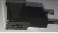
The image right shows a module, it has only one task, supply voltage 5 V, one interface, an USB plug, no more.
The Reset module in Java implements the interface on module level:
//fpga/exmpl/stdmodules/Reset.java
public class Reset implements FpgaModule_ifc, Reset_ifc {
  .....
  @Override public boolean reset ( int time, int max) { return this.q.res; }
It’s very simple: It accesses the variable res in its own inner class q
which is the PROCESS class for the reset functionality.
This is the detail of this Reset module.
The Java2Vhdl translator evaluates this term in the context of this module which is given as reference. Hence the result is the already above shown VHDL code:
      IF (res_Q.res)='1' THEN
          ct_Q.ct <= TO_STDLOGICVECTOR(BlinkingLed_Fpga_time_BlinkingLed);
Generally, only the term of the return statement is evaluated.
If the interface operation contains more statements, it is usable for simulation on Java level.
For the ordenary software execution of interfaces concepts in Java as also other programming languages
the interface operation can also change data and do anywhich else.
But this "full freedom to do whatever you want" is also criticized in some software writing guidelines.
Normally it is a good style to prevent or forbid changes in another software module on only access operations.
Changes should be done with (also maybe interface-) operations which are named set…, do…, process… or exec…
or such else. For that things the processes in VHDL are responsible.
It means execution routines cannot be invoked in the Java context for VHDL hardware descriptions.
But the return expression can be more complex, for example can contain logical combinations, access to bit ranges,
comparison and all what is possible also in other expressions.
This expression is generated inside the accessing PROCESS.
If the same interface operation is used more as one time in different contexts, this operations are generated on any access.
It is similar as execution of the operation in the Java runtime. Also there any access executes the statements again.
It means, the PROCESS of the module can prepare proper signals for simple access if it is expectable that this signals are used more as one time. On the other hand the optimizer while routing can accomplish the aggregation of multiple equal accesses. How these accesses are to be designed is up to the Java description of the VHDL developers.
Now, any module can implement this Reset_ifc. It means for testing, or for another design, you can use another module for the reset signal
without change of the inner structure of the using module. The Java2Vhdl translator gets the correct access.
4.4.4. Interface agents or access instances
 If a module has more interface connections, especially connections of the same type more as one,
then it is not optimal or not possible for the same interface type to implement the interface with the module as a whole.
For that Java offers an interesting possibility:
Implementing the interface in instances of anonymous inner classes.
The inner class has only the task to implement the interface with the possibility to access to the environment (outer) class
which is the module. For that it can be seen as agent which is responsible to access to inner details of the module
from outside, without the necessity to regard this access in the module itself.
On the other hand it can be designated as access point.
If a module has more interface connections, especially connections of the same type more as one,
then it is not optimal or not possible for the same interface type to implement the interface with the module as a whole.
For that Java offers an interesting possibility:
Implementing the interface in instances of anonymous inner classes.
The inner class has only the task to implement the interface with the possibility to access to the environment (outer) class
which is the module. For that it can be seen as agent which is responsible to access to inner details of the module
from outside, without the necessity to regard this access in the module itself.
On the other hand it can be designated as access point.
//fpga/exmplBlinkingLed/fpgatop/BlinkingLed_FpgaInOutput
package org.vishia.fpga.exmplBlinkingLed.fpgatop;

import org.vishia.fpga.Fpga;
import org.vishia.fpga.stdmodules.Reset_Inpin_ifc;

public class BlinkingLed_FpgaInOutput {
.....
  /**Get the reset pin as referenced interface access from a module.
   * Using the {@link org.vishia.fpga.stdmodules.Reset} may be seen as recommended because it clarifies a longer reset signal.
   */
  @Fpga.IfcAccess public Reset_Inpin_ifc reset_Inpin = new Reset_Inpin_ifc () {
    @Override public boolean reset_Pin() { return BlinkingLed_FpgaInOutput.this.input.reset_Pin; }
  };
Such an anonymous class instance or agent is shown here for the access to the reset pin itself.
The pin is located in a static class Input definition in this module with a final Input input = new Input() instance.
This is used to generate the PORT definition in VHDL, but this is not the point of interest here.
For the port definition, especially, there may be a lot of pins. A flexibility is necessary because the same FPGA functionality may be necessary to implement in different environments, different card types etc. For that the interface access to the port pins is a very good idea and reduces adaption effort and error possibilities because of pin confusion.
Hence, the port definition is associated to an own module (which can be replaced for different applications without replacing and adaption of other modules). This module contains:
public class MyPortsVersionXY_FPGA {
  public static class Input {
    //.... input pins
  }

  public static class Output {
    //.... output pins
  }

  public final Input input = new Input();     //instantiation
  public final Output output = new Output();

  //some access operations:
  @Fpga.IfcAccess public Type_Inpin_ifc access_Inpin = new Type_Inpin_ifc () {
    @Override public boolean access_Pin() { .... }
  };
Now this module can be connected with dedicated access instances to any module which needs an input pin. More as that: A module which needs primary an input pin can also be connected not immediately to the pin, but to another module may be with a filter functionality. This other module should only offer also such an interface access agent with the same interface type.
Of course this Port module is only an example. The interface access agents can be used anywhere for more complex applications.
4.4.5. Interface access instances for stubs (replacement for non existing module outputs)
Especially for test, but also for variants of a FPGA design sometimes a functionality is not necessary.
Without adaption of the module, the inputs can be connected to constant signals driving '0' or '1'.
The place and route will be remove this unnecessary parts. But on source level an adaption should not be necessary.
Adequate can be done if some constant values are necessary. The constant values should not be set in a module itself to preserve flexibility, it should be delivered from outside. It’s the same story: a module should not be modified and adapted for a specific use, but the functionality should be defined externally with appropriate connections.
For the Blinking Led example this is done with timing parameters:
//fpga/exmpl/modules/BlinkingLedCt.java
        if(ref.reset.reset(time, 20)) {          // interface access to assigned here unknown reset module
          this.ct = ref.cfg.time_BlinkingLed();
The request is adequate, a value should be accesses. It is not first intendet that this is a constant value. It can be also a signal which contains this reload value as dynamic information.
Especially for tests sometimes signals are terminated by fix values, if this functionality is not in focus yet.
The signals should be fulfilled, of course, but inputs may be always false or '0' for this test condition
or for more simple usage of a module. The last hint is also important:
A module can contain more functionality as necessary for the amount of usages.
If inputs are terminated with constants and outputs are not used, then the routing process will remove this unnecessary parts.
The sources can contain it, without disadvantages.
It means also that a module should not be prepared or adapted for specific usage situations.
It can be uses "as is", and the outer signals and connections determine which is really implemented in the FPGA.
For that all reasons a second use cases and translation goal for interface access is supported by the Java2Vhdl converter:
If the return expression delivers a constant value, then a CONSTANT definition in VHDL is created and used.
Follow the example: The interface to access the time_BlinkingLed() is implemented here in the main or top level file
also with an access instance:
//fpga/exmpl/modules/Fpga_BlinkingLed.java

  /**Provides the used possibility for configuration values.
   */
  @Fpga.IfcAccess BlinkingLedCfg_ifc blinkingLedCfg = new BlinkingLedCfg_ifc ( ) {

    @Override @Fpga.BITVECTOR(8) public int time_BlinkingLed() {
      return 0x64;
    }

    @Override public int onDuration_BlinkingLed() {
      return 10;
    }

    @Override
    public int time() { return 0; }  // set from beginning

  };
The essence is:
The return … expression contains only one term, it is a constant. If this situation is detected,
this constant value is generated in VHDL with the name of the module and the name of interface operation, it`s unique.
The result is (already shown above):
CONSTANT BlinkingLed_Fpga_onDuration_BlinkingLed : INTEGER := 10;
CONSTANT BlinkingLed_Fpga_time_BlinkingLed : BIT_VECTOR(7 DOWNTO 0) := x"64";
The advantage of building a constant element instead the immediately constant value is: It is obvious in VHDL. Elsewhere only the constant value will be written there as evaluation of the expression, and the back tracking to the Java code is difficult.
If for instance inputs are terminated by a constant to prevent usage, the generated VHDL code contains for instance:
CONSTANT Toplevel_Fpga_inputX : BIT := '0';
 ....
PROCESS ...
  IF Toplevel_Fpga_inputX = '1' THEN
    ...
In VHDL you see that the input of the module is used, but the expression is never true. Hence, the router removes this part, proper for the use case.
The idea to implement such termination interfaces on the top level comes from the idea, that the top level, or the whole design decides about usages of details of some modules. Another module as stub is not necessary. It simplifies the design. But of course a specific module can also be used for that.
4.4.6. How does the interface technology works for Java2Vhdl
As you have seen in the chapters above: The references and interface operations are full resolved to simple accesses to the internals of another module. Here a question can be asked: Why is it so complicated to run the programs with virtual operations? The interface usage in Java is the same as virtual or overridden operations with late linkage in C++.
The answer is: If references are not full clarified from beginning, the mechanism of the virtual table is necessary.
This is the common approach for software execution.
But if references are clarified from beginning in the construction phase, and they are never changed,
then the execution level can use the simple immediate access.
It may be also in the same kind for a Java just-in-time (JIT) compiler: This is the translation from Java byte code to machine code on loading a class.
After loading and preparing the immediate machine code is executed. Thats why Java execution needs more startup time, but then it runs fast.
If references are organized as final in the constructor, the JIT can optimize it.
Whereas, C++ has not such an JIT compiler, and should use the virtual operation call anyway.
Now, for the FPGA usage, the references are also clarified from beginning, with the adequate specific constructs also using the init(…).
Hence it can be resolved on translation time.
There are two things to considerate:
-
The refernced module
-
the interface operation.
On translation of each module the interface operations (only in the first level classes of each file, not in inner classes) are gathered. The return statement is searched and evaluated.
Either it is a simple constant, then the constant is stored in the idxConstDef:
-
All constant definitions: J2Vhdl_FpgaData.html#idxConstDef
and the const definition is stored in
-
constant definition of an interface operation: J2Vhdl_ModuleType.IfcConstExpr.html#constVal. Or if it is not a simple constant the expression is stored in
-
expression of an interface operation: J2Vhdl_ModuleType.IfcConstExpr.html#expr
Both alternatives are then stored module-type-related in
-
interface operation per module type: J2Vhdl_ModuleType.html#idxIfcExpr
On translation this table is reported in the -rep:reportfile.txt for this example as:
== J2Vhdl_ModuleType: Reset
  ifcOperation()    | access    {@link J2Vhdl_ModuleType#idxIfcOperation}
--------------------+----------------
  reset()           | this.q..??refres @;
--------------------+----------------
If an interface operation is detected as part of an expression, then the reference is dissolved, detecting the type of the reference, and the interface operation is searched (binary search) in that module type related index.
Then either the constant definition is immediately used, or the given expression is evaluated as any other expression too, whereby the module context is switched.
4.5. Overview modularity
The next image should show the variants in a common way (unrelated to the example), also with public immediately access in the modularity:
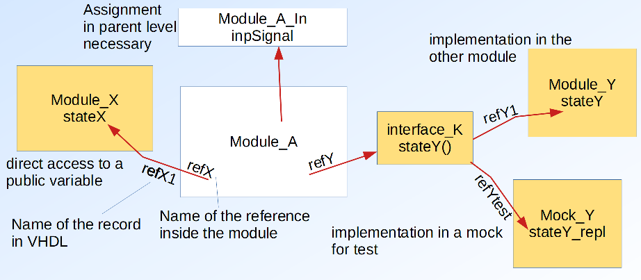
-
The
Module_A_Inin this image is an innerInclass adequate to the VHDL approach usingPORT. It is possible. -
Left side an immediately access to a inner variable in Java is shown. The variable should be
public. The disadvantage for that is, that the whiteModule_Ashould know the defintiion ofModule_X. That is possible and also familiar in Java. It is bad for module test, because on testing also an instance of theModuleXshould be present in the test environment, exact this module or a replacement but with the same package path, which is terrible for source maintaining (version management). -
But also for that immediately usage the inner aggregation
refXis translated to theref1on usage. It means the type should be known, but the instance is determined outside. This is important if more as one instance for one type is existing. -
Right side the interface usage is shown. The interface operation should have the same name as the accessed variable. That is not necessary from the view point of Java. It is necessary for the Java2Vhdl translation. But it is possible.
-
You can connect different implementation modules also on FPGA level in VHDL. It means the variable
stateYcan exist in different records types. Only the name is determined. -
Now the advantage for testing is shown. That is only done in Java, not on VHDL level. That’s why the test implementation of the
interface_Kcan use any implementation, should not access exact one variable. -
Note that also for the module implementation for Vhdl translation the access operation here for
stateYcan contain more as the simple access to the variable, for example log informations, adaption, a debug break point. That is all possible on Java level, not translated to VHDL. For VHDL anytime the simple access to the record signal with the same name as the access operation is translated.
5. Including existing VHDL files
There are two reasons to include a given VHDL file in the generated sources:
-
a) Existing reused modules
-
b) Often the tools for FPGA design have features to generate VHDL files for specific features, for example for a RAM block.
VHDL is the standard for FPGA design (beside Verilog), hence VHDL is necessary to include.
For simulation on Java level, the functionality of the VHDL code should be emulated. For example for a RAM module this should be simple. You may also only simulate only the basically functionality to fulfill the interface to the module.
5.1. Java class which emulates the given VHDL file
The Java class for the given VHDL file to include it in the Java sources should start with the annotation:
@Fpga.VHDL_MODULE(vhdlEntity = "Vhdl_filename") public class EmulationClass implements FpgaModule_ifc {The class emulates the behavior of the included VHDL file, maybe only in basically features.
The name of the EmulationClass and the name of the Vhdl_filename should be the same or similar
to find the coherence. But because that are different name approaches it can be slightly different.
The port definition in the Emulation class should be written following the port definition in the orginal VHDL file, for example:
  public static class Input {
    public @Fpga.STD_LOGIC boolean Clock;
    public @Fpga.STD_LOGIC boolean ClockEn;
    public @Fpga.STD_LOGIC boolean Reset;
    public @Fpga.STD_LOGIC boolean WE;
    public @Fpga.STDVECTOR(7) int Address;
    public @Fpga.STDVECTOR(8) int Data;
  }

  public static class Output {
    public @Fpga.STDVECTOR(8) int Q;
  }

  public Input input = new Input();
  public Output output = new Output();
This is for the example with the RAM block VHDL. See next chapter for VHDL result:
The rest of the class file contains the emulation of the functionality in any desired kind,
for your own and responsible, without influence to the Java2VHDL translation.
The step(…) and the update() operation should be overridden from the FpgaModule_ifc
as given in the class definition and due to the general approaches for simulation.
5.2. Definition of the module
The external VHDL file should be included with its emulation class as module in the :
  class Modules {
    ....
    public final EmulationClass vhdlModuleName = new EmulationClass();
Because of the annotation @Fpga.VHDL_MODULE(vhdlEntity = "Vhdl_filename")
the definition of the VHDL component is included in the generated VHDL file, due to the example above:
-- The external VHDL file RAM_SpiRamSel is defined here.
--  Its file and entity name comes from annotation "@Fpga.VHDL_MODULE ( vhdlEntity = <name> in the Java implementation file.
--  The PORT variables comes from the implementation Java file, which should match to the VHDL file.
COMPONENT Vhdl_filename
PORT (
  Clock: IN STD_LOGIC ;
  ClockEn: IN STD_LOGIC ;
  Reset: IN STD_LOGIC ;
  WE: IN STD_LOGIC ;
  Address: IN STD_LOGIC_VECTOR(6 DOWNTO 0) ;
  Data: IN STD_LOGIC_VECTOR(7 DOWNTO 0) ;
  Q: OUT STD_LOGIC_VECTOR(7 DOWNTO 0)
 );
END COMPONENT;
5.3. Usage of the module
For usage of the module in a Java2VHDL generated Java source it needs an inner class with annotation:
@Fpga.LINK_VHDL_MODULE private static final class Vhdlink_vhdlModuleName {The class name should follow the instance name of the Vhdl module in the class Modules { ….
The instance of this class (with same name with lower case first char)
is responsible to exact this vhdl module, hence this naming convention is acceptable.
But the class name should start with Vhdlink_ and hence
the two instances for step() and update() with vhdlink_.
This class can have some interim variables to organize the mapping, for example:
    @Fpga.STDVECTOR(8) final int ramData;
    @Fpga.STDVECTOR(7) final int ramAddr;

    Vhdlink_vhdlModuleName() {
      this.ramData = 0;
      this.ramAddr = 0;
    }
The default constructor is for simulation only. It is the 0-set adequate "reset" in the hardware.
The here defined variables are assembled in a record and SIGNAL record definition, adequate to the example:
TYPE Module_Vhdlink_vhdlModuleName_REC IS RECORD
  ramData : STD_LOGIC_VECTOR(7 DOWNTO 0);
  ramAddr : STD_LOGIC_VECTOR(6 DOWNTO 0);
END RECORD Module_Vhdlink_vhdlModuleName_REC;

  .....

SIGNAL module_Vhdlink_vhdlModuleName : Module_Vhdlink_vhdlModuleName_REC;
That are combinatoric values.
Inside the class the constructor should be written in the following kind (example):
    @Fpga.LINK_VHDL_MODULE Vhdlink_vhdlModuleName(int time, EmulationClass vhdlMdl, Modules modules, Ref ref, Module thism) {
      this.ramAddr = Fpga.getBit(ref.dcmd.wrSelectSpeSlaveToTx(), 15) ? Fpga.getBits(ref.dcmd.wrSelectSpeSlaveToTx(), 14, 8) : Fpga.getBits(thism.frameSelect.ctData,9,3);
      vhdlMdl.input.Clock = Fpga.clk;
      vhdlMdl.input.ClockEn = ref.ce.ce0();
      vhdlMdl.input.Reset = ref.res.reset(0, 0);
      vhdlMdl.input.Address = this.ramAddr;
      vhdlMdl.input.Data = Fpga.getBits(ref.dcmd.wrSelectSpeSlaveToTx(), 7, 0);
      vhdlMdl.input.WE = Fpga.getBit(ref.dcmd.wrSelectSpeSlaveToTx(), 15);
      vhdlMdl.step(time);
      vhdlMdl.update();
      this.ramData = vhdlMdl.output.Q;
    }
The constructor works in the same time as in other processes with annotation @Fpga.VHDL_PROCESS:
In the step(…) routine of the module class a this.ram_d = new Ram(…) will be created,
and in the update the this.ram = this.ram_d; new instance is established for usage in the next step.
As one argument of the constructor EmulationClass vhdlMdl with the name vhdlModule
the type of the emulation class is necessary for construction. This type is used from the Java2Vhdl translator
to search the emulation class, and get its entity and file name of the VHDL file
from its annotation @Fpga.VHDL_MODULE ( vhdlEntity = "<name>" ) (see above).
That is used as type name of the PORT MAP.
For simulation the step(…) and update() of the @Fpga.VHDL_MODULE public class EmulationClass…
is called one after another.
The isolation from step() and update() for a correct simulation execution is done by storing the result value
of the VHDL module here in the ramData internal data,
which is accessible only after the update() from the wrapping @Fpga.LINK_VHDL_MODULE("ram").
Be aware that assignments are only regarded till the step() operation (following by update()).
After step() assignments to the local variables of this class stores the result of the linked modules.
That is because in VHDL in PORT MAP only an assignment between the in/out variables of the called module
to local variables can be associated, not expressions.
Necessary expressions to build the correct input values are before step,
necessary expressions to work with the output variables are only possible as access to the intermediate variables.
The translation to VHDL code produces the following for this example:
-- The external VHDL file RAM_SpiRamSel is included here.

-- Assignments for VHDL instance inputs:
txSpe_Ram.ramAddr  <= TO_STDLOGICVECTOR(data_Data.wrSelectSpeSlaveToTx(14 DOWNTO 8))  WHEN data_Data.wrSelectSpeSlaveToTx(15)='1' ELSE txSpe_FrameSelect.ctData(9 DOWNTO 3) ;

-- <name>: <type>
--   ... <name> is build from <moduleName>_<className> with annotation "@Fpga.LINK_VHDL_MODULE"
--   ... <type> is gotten from the Java class implementation annotation "Fpga.VHDL_MODULE ( vhdlEntity = <type> )"
module_Vhdlink_vhdlModuleName: Vhdl_filename
PORT MAP(
  Clock =>  TO_STDULOGIC(clk) ,
  ClockEn =>  TO_STDULOGIC(rxClkSync_Q.ce0) ,
  Reset =>  TO_STDULOGIC(reset_Q.res) ,
  Address =>   txSpe_Ram.ramAddr ,
  Data =>  TO_STDLOGICVECTOR(data_Data.wrSelectSpeSlaveToTx(7 DOWNTO 0)) ,
  WE =>  TO_STDULOGIC(data_Data.wrSelectSpeSlaveToTx(15)) ,
  Q => txSpe_Ram.ramData
 );  --PORT MAP Vhdl_filename
The comments in the VHDL file should show the coherence to the Java sources. The Assignments are only generated if there are intermediate variables.
The Vhdlink_… class should be instantiated and used for step(…) and update(…)
in the same kind as a process class:
public Vhdlink_vhdlModuleName vhdlink_vhdlModuleName = new Vhdlink_vhdlModuleName();
private Vhdlink_vhdlModuleName vhdlink_vhdlModuleName_d;

  ....
public void step() { //step from the module
  ....
  this.vhdlink_vhdlModuleName_d = new Vhdlink_vhdlModuleName(this.vhdlink_vhdlModuleName, modules.vhdlModuleName, ....)
....
public void update() { //update from the module
  ....
  this.vhdlink_vhdlModuleName = this.vhdlink_vhdlModuleName_d;
The update assures as for processes that the Java simulation uses the new data in the next step only (clocked).
It is obviously that the instance of the vhdlModuleName is associated here to the vhdlMdl calling argument.
But this is not obviously by the Java2Vhdl translation process, only for simulation.
That’s why it needs the naming convention, the organization class Vhdlink_… should follow the vhdl module name.
6. State machines, enum
State machines are familiar both in software and in hardware. In software solutions often the so named "Harel-Statecharts" are used. (https://en.wikipedia.org/wiki/David_Harel), which defines nested and parallel states with history. That’s a part of the "Unified Modeling Language" (UML): https://en.wikipedia.org/wiki/UML_state_machine, definition by omg.org: http://www.omg.org/spec/UML/. For Software state machines often events are responsible to switch the states.
But all these practical things are not substantiated in the Java core definition. It is possible in Java, but with specific classes.
Hardware state machines are often a little bit simpler. Especially there are not event driven, the system clock switches because of conditions. But the idea of nesting and parallel states is and should also possible and practicable. Also the idea of the event may be possible, presented by an additional condition (the event bit). This means that thinking in terms of states should not distinguish too much between software and hardware.
A basis for this is the enum definition for states and the enum type for the state variable. Exactly this is implemented in the current version of Java2Vhdl.
6.1. State variable with 1-of-n decoding
A state variable is basically a numeric value. For 5 states you need 3 bits to code numbers between 1 to 5 as presentation of the state. But another coding is better:
Use 5 bits if you have 5 states, the state variable is 1-to-5 decoded (one bit from 5 is set).
00000 invalid state
00001 state A
00010 state B
00100 state C
01000 state D
10000 state E
With this coding schema only one bit is need to detect a specific state, and this is a lesser effort in routing, for the FPGA hardware resources. The number of FlipFlops in a FPGA are usual enough, the scare resource is often the lines for routing and the look up tables (LUT) for combinatoric.
Only the quest of the invalid state (after reset) needs testing of all 5 bits, or more for more states. In the current version of the Java2VHDL translator, the set of a state influences all state bits. Most of them are set from 0 to 0, only the elapsed state bit is set from 1 to 0 and the new state bit is set from 0 to 1. Maybe the router can improve this situation by optimizing. Setting all state bits clarifies a possible mistake if more as one bit is set.
6.2. enum definition in Java
Known from C/++ language, a enum is only a definition of an integer constant value by a symbol, and the enum type assures only acceptance of these enum constant definitions. In Java the enum definition is a little bit more powerful:
-
Java creates an enum Object with some values as constant.
-
The enum value in an enum variable is the reference to one of these enum constant objects. This needs 8 byte for a pointer, in opposite to C/++ where for example 2 Bytes for an
int16_tenum base type are sufficient. But Java runs only on powerful processors, not an disadvantage.
The first point offers usage of some more properties of the enum constant.
  /**States for xyz*/
  public enum MyState {
    Undef  (0b00000, -1, '0'),
    /**State A */
    A  (0b00001, 0, 'A'),
    B  (0b00010, 1, 'B'),
    C  (0b00100, 2, 'C'),
    D  (0b01000, 3, 'D'),
    E  (0b10000, 4, 'E'),
    ;
    public final int _val_;
    public final char show;
    final int bit;
    /**Constructor for the enum value
     * @param value The internal used Vhdl value
     * @param bit the bit number for VHDL translation, following the value
     * @param show character to show the state in println
     */
    MyState(int value, int bit, char show) {
      this._val_ = value; this.bit = bit; this.show = show;
    }
  }
This is a strikingly example. The state names A..E are of course any identifier,
but you have a namespace inside the enum definition (clashs are prevented, better than in C/++).
The fields value and bit are required. The field show is proper usable for output of test results,
see some programming examples. The state Undef is the undefined state after reset.
6.3. state variable as enum
The state variable in Java has this enum type. Concluding, Java assures only set with a valid state value.
For the VHDL conversion it should be a bit vector (not a STD_LOGIC_VECTOR, not supported in the current version).
A BIT_VECTOR is sufficient for usage.
@Fpga.BITVECTOR(5) final MyState state;The number of bits should follow the enum definition, elsewhere mistakes in the generated VHDL code are resulting.
6.4. query state variables
The query is usal written as:
  if( z.state == MyState.Undef ) {
    //.....
  else if( z.state == MyState.A ) {
    //.....
  else if( z.state == MyState.B && otherSignal ) {
    //.....
As you see, the content of the state variable is compared to the given state constant value.
Usage of the identifier of the enum type definition is necessary in Java, it clarifies name clashing
and increases obviousness and readability.
Usage of switch … case is possible and may be also recommended in Java, but it is not yet supported in the Java2Vhdl translator.
As given in the third query line the query of the state can be also combined with the logic relation to other signals (variables),
which are the conditions for state usage. This is better possible in an if (… construct.
The Java2Vhdl translator detects a definition of a state constant with a bit value >=0, then only the query of the state bit is produced in VHDL. For this example the result in VHDL is:
  IF(module_Prc.state = Module_MyState_Undef) THEN
    --.....
  ELSE IF ( module_Prc.state(0)='1') THEN
    --....
  ELSE IF ( module_Prc.otherSignal AND module_Prc.state(1))='1' THEN
    --....
The first comparison of state used the state value 0b00000 which is not marked with a valid bit,
hence the Java2VHDL translator generates a full comparison of the state vector with the constant value which is defined as
CONSTANT Module_MyState_Undef : BIT_VECTOR(4 DOWNTO 0) := "00000";The second comparison knows from the Java enum definition, bit 0 is associated,
and generates the simple access to this bit value.
The third query combines the BIT access to the state BIT_VECTOR bit with the BIT variable otherSignal
as BIT-AND and converts outside of the paranthesis to the necessary boolean value for the IF query.
myBitVariable = (z.state == MyState.C) & otherBitVariable;This is a combinatoric from a state query and a boolean, it is translated very simple to:
module_Prc.myBitVariable <= module_Prc.state(2) AND module_Prc.otherBitVariable;It means it is only a BIT logical combination.
6.5. set state variables
To switch the state only the new state should be set:
    if(condition){
      this.state = MyState.C;
This is immediately translated to
    IF condition THEN
      module.Prc.state <= Module_MyState_C;
It means all state bits are determined. The optimizer of the FPGA routing process may detect not changed bits.
6.6. Nested and parallel states
As mentioned in the introduction, Harel-Statemachines have nested and/or parallel states. Especially nested states helps get overview, it follows the practical requirements.
In Java level for VHDL any sub state in a state should have its own state variable. Entry in a nested state needs set two state variables. Query of the composite state (the outer of nesting) queries and set only the outer state variable, the inner state remains its value. This is helpful for the entry to the "history state", to the given remained inner state back again.
These things are all able to do on user level. A translation between UML diagrams with given Harel state charts to Java and then to VHDL may be nice and possible, but not presented here. See links in german:
7. Timing constrains for place and route
The next examples are related to the Lattice Diamond tool. Whether constrains should be given in the same syntax form for other tools (Xilinx & co) is not yet clarified.
See also basic considerations in the chapter Timing constraints for CE and steadyState
Simple, the whole FPGA design should have the same clock. That is a basic mentioned in chapter Principle of functional simulation of synchronous state machines, and it makes sometimes easier to manage timing and functionality. But this is precisely why a higher clock frequency is usually used as the base clock, even though certain functions can operate in slower cycles.
The basic in VHDL for this use case is:
--From example: BlinkingLed_Fpga.vhd
ct_Q_PRC: PROCESS ( clk )
BEGIN IF(clk'event AND clK='1') THEN

  IF ce_Q.ce='1' THEN
  --.... logic working only if ce is set
  END IF;
It is a clock enable strategy. The Flipflops remains unchanged if ce='0'.
The adequate form in the Java src is similar:
//fpga/exmpl/modules/BlinkingLedCt.java
    @Fpga.VHDL_PROCESS Q(int time, Q z, Ref ref, Modules modules) {
      Fpga.checkTime(time, ref.clkDiv.q.time, 1);  // for the ce signal, constraint with 1 clock delay.
      if(modules.ct_clkDiv.q.ce) {
        Fpga.checkTime(time, z.time, 20);        // check whether all own process signals are persistent since 20 time steps.
        Fpga.checkTime(time, ref.cfg.time(), 20);// check all signals from the referenced module.
        this.time = time;                        // all variables are declared as possible set with this time stamp.
      //.... logic working only if ce is set
    }
Supposed, this ce signal comes with a cycle of 200 ns as in the example, you can write a constrain
in the lpf file of the lattice Diamond tool:
PERIOD PORT "clk" 10.000000 ns ;
MULTICYCLE FROM GROUP "ct_q" TO GROUP "ct_q" 20.0 X;
It means that the routing regards the basic clock frequency of 100 MHz or 10 ns cycle,
but between the members of the GROUP "ct_q" the timing path can have till 16 times slower, 160 ns.
With this information the place and route tool can route firstly the fast paths, then with the remaining resources the slower paths.
The place and route tool is specialized for that requirement.
In result you have a proper routing result without timing violations if your requirements to timings are not too hard.
But it is precisely because slower paths are allowed, because the possible cycle is slower, that this is possible.
But the remaining quest is: How to build the groups?
Here the Java notification and the test at Java level helps.
The Fpga.checkTime(…) statements are evaluated. The second argument is the time variable in the group, it designates the source group.
The destination group is the from the own process. The constrain is the third argument, as mulitply of clock cycles or steps in the simulation.
If the same constraints are detected with different Fpga.checkTime(…) statements, then of course these groups can be combined.
Also using an interface access (see chapter Interface technology in Java for VHDL allows the assertion with the access time. This is the importance for module interconnection:
//fpga/exmpl/modules/BlinkingLedCt.java
        if(ref.reset.reset(time, 20)) {          // interface access to assigned here unknown reset module
          this.ct = ref.cfg.time_BlinkingLed();
The first argument is the current time, the second one the maximal delay. The check itself is (should be) done in the interface implementing operation,
for the simulation. The constrain generator does not recognize it. It does regocnize the interface access with this two arguments.
The source time group is the referenced module (left of interface call, here ref.reset with the resolving of the reference to the real module.
The desination time group is the own, the constrain is the second argument.
In the version 2022-05 the time constrains are not yet automatically generated, this is todo in the nearer future. But the constrains are used for simulation, manuall written than for the place and route.
8. Test
The Test of the logic is a very important part.
General a test should be done in two categories:
-
Test under exact defined conditions expecting dedicated results. This is important for two situations:
-
Test of features which are assumed in requirements.
-
Repeated tests after changes to fast and automatic clarify, all is ok.
-
-
Test under accidently conditions. This tests are important to study the behavior independent of planned tests and exactly defined requirements.
-
It is possible that some conditions are not exactly defined, but that definitions should be intrinsinc necessary.
-
Furthermore, the tests should be done in three situations:
-
Test of the ready to use logic in the routed FPGA under several conditions (several input signals), of course in both categories as above presented, planned tests and accident tests (sometimes denoted by "white noise tests").
-
Test of the whole logic on Java level with dedicated test cases, or maybe also for accident inputs. Whereas a random value generator may be used in software. But of course the accident situations follows only the programmed randomizations, this is not a "white noise test".
-
Test of modules ("unit test"). Usual for that only planned tests are determined. The behavior of a module should follow exactly situations, this follows the denotation "design by contract". The contract of the behavior of a module should be well defined. A module should be manageable (rather than a complex system).
These are pure basics about tests that are generally applicable.
8.1. step and update operations
The content of the step(int time) and update() operations are not used for the VHDL translation.
Essential for the VHDL translation are only the existence of the inner classes designated by the annotation @Fpga.VHDL_PROCESS
in the modules and the instantiation of the modules in a class Modules in the top level file and also possible in modules for sub modules.
It means the (manually programmed) content of this routines should follow the existing module instances and process classes. Then only the behavior of the test is identically with the original FPGA behavior. It means, intrinsic, this operations should be generated also for Java level. But this is not done yet.
The step routine prepares the states before the next clock. The update routine is the clock, it is the manifestation for the next state.
8.2. Input signals for test simulation in Java
If you are testing the whole FPGA design usual the top level file has a Input and Output inner class
with the designated input and output instance which presents the pins of the FPGA.
Hence should only set the elements of the input with the appropriate values.
This input values can come from simple test bed algorithm, or from more complex algorithm maybe also fet from values in tables,
the test cases.
If you are testing a module usual the module has interface connections. You should satisfy this interface requirements by implementations in the test bed, for the appropriate input signals.
8.3. Output signals for manually evaluation of the test results
With given tools of FPGA simulation a graphical output is usual for instance:
Of course an adequate approach is possible for Java simulation because Java has graphical possibilities, it can be programmed in a specific way, or given routines in libraries of from other tools are usable. But is this the best one?
The very simple solution presented below may be also satisfactory:
ct.ctLow__________:0001 0000 ffff 61a7 ...0001 0000 ffff 61a7 ...0001 0000 ffff 61a7 ...0001 0000 ffff 61a7 ...0001
ct.ct_____________:63   63   63   62   62      62   62   61   61      61   61   60   60      60   60   5f   5f
ct.time___________:                    '5.001.20              '10.001.40             '15.001.60             '20.001.
io.ledA___________:_____________________________________________________________AAAAAAAAAAAAAAAAAAAAAAA_____________
io.ledB___________:_________________________________________________________________________________________________
=========================================================================
ok Test_BlinkingLed
This is the content of a simple text file, able to view with any normal stupid or better a powerful text editor, for example https://notepad-plus-plus.org/ or http://www.jedit.org/. The original lines produces by the Blinking_Led example has a length of ~5000 character, no problem for viewing, shifting and copy also a part to the clipboard using the "rectangular selection" mode in Jedit or the "column selection mode" on Nodepad++.
The lines are time lines. Each column position in each line presents the same time, more exact the start column of a longer information. Of course you should use a monospace font in the editor.
The resolution of such an output can be one system clock per column or character, or also condensed, for example a dedicated CE (clock enable) occurrence per column.
Because you can use proper characters to show a state, this is more obviously as only simple lines. Especially you can assemble more signals in one line using proper characters. For that look on a snippet of another example:
rx2.rxCE___________:____________----f---------f---------f--=======e=========e=========e==++++e++++++e++++++e++++++e++++________________
Time.time__________:^``8.54      |      |      |      ^``9.00       |      |      |      ^      |      |      |      |      ^``10.00
This first line shows three signals:
* The 'f' or 'e' is a special clock enable signal, always one clock period wide.
* The _ is used for the idle state, then also no ce should be occur.
* The --- is one specific state, in this state a ce may occur as shown for the one clock period.
* The === and + is each another state, also with occurrence of ce.
The letter for the occurrence of the ce signal is also changed for better visibility.
To build this output, you should override the operation addSignals in the derived class of
org.vishia.fpga.testutil.TestSignalRecorder
in the following form:
char ce;
if(thism.qrx.ce) { ce = thism.qrx.dataState ? 'e' : 'f'; }
else if(thism.qrx.stateA && thism.qrx.stateB) { ce = '='; }
else if(thism.qrx.stateA) { ce = '-'; }
else if(thism.qrx.stateC) { ce = '+'; }  //(not all is full decoded)
else { ce = '_';}
this.sbCe.append(ce);
You can use more mnemonic character for the states, and also for short signals in the state. The only one challenge is, a good documentation of the used characters. You get a very compressed representation with more expressiveness than many lines.
The second line shows the time, which is equidistant here. This signal is created using a instance of
Using this class, the time is always written on start of line, and then in a proper distance with 5- and 10 divisions.
The time in the line may not be equidistant, depending of the output routines.
This is an advantage. You can show an incident in detail zoomed in time, whereas non interesting time spreads are condensed.
The example shows it. The trigger for writing details is here the ctLow with the value 0x0001. It is shortly before zero crossing.
The ct, the higher count is shown, its value changes if the ctLow reaches ffff and the reload value is also set if ffff is reached before,
and not as expectable, if 0000 is reached before. This is the written logic.
The time is also presented, only on end of this zoomed spread because it needs upto 13 character positions.
The time is a millisecond value, proper readable till 10 ns resolution.
As you can see the period of one count step of ct is not 5.00000 ms as expected than 5.00020 ms, 200 ns longer.
This is an effect which is better able to see with this numeric time information than in a diagram with measurement.
The algorithm in Java to sort the output for this information is not complicated:
//fpga/exmpl/modules/BlinkingLedCt.java
    @Override public int addSignals ( int time, int lenCurr, boolean bAdd ) throws IOException {
      BlinkingLedCt thism = BlinkingLedCt.this;
      int zCurr = this.sbCt.length(); // current length for this time
      int zAdd = 0;                   // >0 then position of new length for this time
      if(thism.ref.clkDiv.q.ce) {       // because the own states switches only with this ce, the signals should also recorded only then.
        if(thism.q.ctLow == 1) {        // on this condition
          this.wrCt = 5;              // switch on, write 5 steps info
        }
        if(--this.wrCt >0) {          // if one of the 5 infos shouls be written:
          StringFunctions_C.appendHex(this.sbCtLow, thism.q.ctLow,4).append(' ');    //append info
          StringFunctions_C.appendHex(this.sbCt, thism.q.ct,2);                      //append info
          if(checkLen(this.sbtime, zCurr)) {      // add the time information if here is space.
            StringFunctions_C.appendIntPict(this.sbtime, time, "33'331.111.11");   // append time info
          }
          zAdd = this.sbCtLow.length();  //length of buffers for new time determined by the sbCtLow, the longest entry.
        }
        else if(this.wrCt ==0) {         // end of the 5 steps, append .... as separation
          this.sbCtLow.append("..... ");
          zAdd = this.sbCtLow.length();  //length of buffers for new time determined by the sbCtLow, the longest entry.
        }
      }// if ce
      return zAdd;       // will be used in TestSignalRecorderSet.addSignals(zAdd) to set all lines to this length
    }//addSignals
Generally for this example, adding a signal is only done if clkDiv.q.ce is true, because:
This module changes only its state with this ce clock enable.
It saves calculation time if this is quest firstly.
Then the trigger for the output is mdl.q.ctLow == 1. With this condition the next 5 ce times are presented.
Because 5 characters are appended to sbCtLow, this is the longest appendix, all lines are elongated to this legth, as you can see in the ouput.
It means this time uses 5 column positions in the output, in all output lines.
You should not see the effort to program the output, you should see the advantage to design your necessary output for complex signals and test cases. Programming in Java is much easier and safer than, for example, in the C++ language or in certain scripting languages often used for simulation tools. You can make extensive use of auto-completion during editing, you will get immediately writing mistake messages (syntax errors) and hints for correction.
This horizontal output as also a vertical output, the time is continued in the lines than in columns, is organized by two classes
in the package org.vishia.fpga.testutil. It is explained in detail in Java2Vhdl_TestOutput.html and for the Blinking Led example
in chapter Java2Vhdl_ToolsAndExample.html#JavaSrcTest
8.4. Test of modules or the whole design on Java level
In Java programming also the environment, the "test bed" should be written. In this test bed the inputs are determined and the outputs are gathered maybe in lists appropriate to states and times. This results can be compared with expected results in a very more proper way because Java is a safe and familiar language.
You can use several test environment approaches. It is recommended to use the simple org.vishia.util.TestOrg,
see ../../../Java/docuSrcJava_vishiaBase/org/vishia/util/TestOrg.html
Last not least the link to the so named StimuliSelector should be also offered here:
This tool is not used yet for the FPGA test, but it is possible. It is used yet for Simulink tests, for algorithm tests in C/++, see ../../../emc/html/TestOrg/testStrategie_en.html#testStrategies and more.
9. Writing style of logic - data assignment versus situation thinking
It is a general question, orientation to data assignment or situation evaluation. What is meant by this?
-
Situation evaluation: Programming is a familiar idea of program flow. The typical construct is
if … then … else. "If a situation is given, then do this and that". This is also the prevailing mindset for VHDL and for the programming style of the 1980th (before Object Orientation became really familiar). -
Orientation to data assign: The real truth of programming is: Influencing data. That is also one of the ideas of Object Orientation. The objects are the data. Program flow and operation is only a way to influence the data. The quest is the state of data. The flow is only a mediator for action.
In graphical models such as Simulink or Labview immediately a data flow is modeled. This is a data flow between function blocks, another level, nor related here. This data flow concept seems to be in opposite to the modeling with UML, which shows not a flow but data relations especially in Class- and Object Diagrams.
Another topic is functional programming. This is more oriented to data assign because all is result of a function, and a function is the result of the input data. This is mentioned here only as additional information.
Look on examples for Situation evaluation versus Orientation to data assign:
9.1. Style: Situation evaluation, program flow
 if(condition) {
   data = changed;
 } else if(other_condition) {
   data = other_input;
   other_data = changed;
 }
Here it is not clarified whether the data are changed anywhere other too,
as well as the other_data are changed in one of the given situation.
The change of data are not well described.
But the reaction of situations (test a condition) is well described.
Usual the condition is only tested one time.
9.2. Style data assignment orientation (data flow)
 if(condition) {
   data = changed;
 else if(other_condition) {
   data = other_input;
 } else {
   //comment: data remain unchanged.
 }
 if(other_condition) {
   other_data = changed;
 } else if(specific_condition) {
   other_data = specific;
 } else {
   //other_data unchanged in all other situation
 }
Here we have two program blocks, because two different data are handled.
The data are not related, except one other_condition influences both.
But the conditions are secondary.
Each program block for one data should be complete for this data.
The disadvantage of data assign orientation: Usual it needs more code. The test of conditions are programmed more as one time. For all data extra. That needs also more runtime for the program in a controller (if the compiler does not optimize).
The advantage of data assign orientation is: The program clearly shows, how data are changed. If one looks on the part for one data specification, it is complete. The data will not be changed anywhere else.
In practice, both approaches are often combined. Fundamental situation as "clear", "reset" are programmed with the situation approach: "what’s happen on clear:…". But for details the data orientation should be better.
The argument of longer execution time is not applicable for the hardware design if complex combinatoric are stored in intermediate variable. If that is not done, the router may optimize the combinatoric too. Only the readability of the code is decisive.
9.3. Ternary or condition operator in Java: condition ? a : b
Now, for thinking to data orientation, in Java (as also in C/++ the so named ternary or condition operator can be used:
data = condition ? changed : other_input;
This is the simplest form with two variants. It can be more complex:
data = condition ? changed
     : other_condition ? other_input
     : data;
This is the same effect as the if in the examples above.
But it is well obviously. Also the else branch is exactly determined.
The compiler of software languages will remove the unnecessary assignment
for the unchanged data.
For this situation it is well documented that the data are used unchanged.
In Java you can use a final keyword for such data:
final int data = condition ? changed
               : other_condition ? other_input
               : old_data;
This is similar as https://en.wikipedia.org/wiki/Functional_programming functional programming. With the final keyword the compiler has more capabilities to optimize.
And now, for hardware design:
The new state of a FlipFlop or a FF group is complete determined by such an final functional construct. The logic is obvious at a glance.
9.4. Solutions for pure VHDL
As mentioned above, VHDL was created in a time (1980th) where structured programming was familiar.
Additional to the known if … then … else … end if; VHDL knows:
-
'case 'selection
is whenchoice⇒statements
This is also typical for situation thinking. The statements can contain any assignment. The selection describes which situation is checked. -
assignment
⇐value1whencondition1
value2whencondition2
elsevalueelse;
This is exactly the behavior for the data assignment thinking. Only one variable is under consideration. It is set under several conditions.
This when … else statement was introduced also for using in processes
(behavioral programming) with VHDL-2008. It is ideal for this case.
But unfortunately VHDL-2008 doesn’t seem to be considerate by all tools and all thinking:
4. Try to only use when else outside a process even though it’s supported in VHDL-2008. Why? Because in 2020, some synthesis tools still have some bugs compiling VHDL-2008. Perhaps in the future this won’t be an issue. Plus, if you have to support an older FPGA using older tools, you won’t have 2008 as an option. Keep these issues in mind when you code. There are better options than when else if you need to have it in a process, like using case instead.
It means it is not able to use for a tool independent translation from Java.
9.5. Java2VHDL for condition operator
Hence, conclusion, in processes only IF can be used for translation of the Java condition operator.
 //Java:
 data = condition ? changed
      : other_condition ? other_input
      : data;
is translated to:
 IF condition THEN data <= changed;
 ELSIF other_conditon THEN data <= other_input;
 ELSE data <= data;
 END IF;
whereas the last line can be removed. This is the same behavior as written with the conditional operator in Java.
What is obviously: The same left side term for the data assignment (data ⇐) is written for each branch.
But this is not an disadvantage. It is readable, and the router and simulation tools with VHDL can proper deal with it.
Only the readability of the source is a little bit not optimal because one line may contain a writing mistake.
But because it is generated code - no problem.
Unfortunately outside of a process IF THEN ELSE cannot be used,
here the WHEN construct is used for translation of such an conditional expression.
The same problem occurs on conversion of a bit in BIT logic from STD_LOGIC:
  -- in a PROCESS:
  IF myBitValue = '1' THEN myStdValue <= '1';
  ELSE myStdValue <= '0';
  END IF;
and outside of a PROCESS
myStdValue <= '1' WHEN myBitValue = '1' ELSE '0';
9.6. Multiplexer in hardware design, problem of WHEN ELSE
In Java it is very simple to write in an expression:
boolean q = a & (b ? c : d) | e;
In this case `c` and `d` is multiplexed by selecting with `b`. The rest is boolean logic.
In VHDL theoretically a
c WHEN b='1' ELSE d
is existing. It works outside of a process. But this construct doesn’t seem to be considerate by all tools and all thinking:
4. Try to only use when else outside a process even though it’s supported in VHDL-2008. Why? Because in 2020, some synthesis tools still have some bugs compiling VHDL-2008. Perhaps in the future this won’t be an issue. Plus, if you have to support an older FPGA using older tools, you won’t have 2008 as an option. Keep these issues in mind when you code. There are better options than when else if you need to have it in a process, like using case instead.
It means, the simple expression for a multiplexer, which is familiar in hardware, is not possible for VHDL.
But instead, VHDL likes to see IF constructs:
IF b='1' THEN t = c; ELSE t = d; END IF;
This works also in processes, it is a basic, supported, known. But what is the disadvantage: As part of an expression we need a temporary variable. And this part of expression should be extracted as extra statement.
  PROCESS
  -- Java: boolean q = a & (b ? c : d) | e;

  SIGNAL b_sel : BIT;  --process variable
  BEGIN
  IF b = '1' THEN b_sel := c;
  ELSE b_sel := d; END IF;
  q <= (a AND b_sel ) OR e;
This complicates the readability. But we have VHDL, the best and safe language for hardware.
9.7. Programming in loops
Also VHDL knows loops. If you following https://vhdlguide.readthedocs.io/en/latest/vhdl/behave.html#problem-with-loops then loops should not be used.
In software two types of loops should be well distinguished:
-
Classic loops for repeated execution till a condition is met. It is typical a
whileloop, orrepeat - until. -
Loops only to execute an algorithm for all given instances. That is not really a execution in the loop, it is only written as loop in software to process all given instances. This can be done also parallel and also sequentially. But because the instances are contained in a so named container the loop works for all member of the container. This is typically a
foreachloop. In Java it is written as:
 //Java
 for( Type element : container ) {
   //do for all element.
 }
Such constructs are parallelizable also in software, for example distributed on several cores of a processor. Why: Because all operations which are executed in a loop one after another are independent. It means the order of execution is not important.
This scheme can now be used for hardware designs for parallelization. Of course the FPGA should have enough resources for the task.
It is also interesting that each element in a container can have a different derived type. It means really, different operations are executed (via virtual operations). Now, thinking in hardware: You have a planned container with elements, the elements are a little bit different and you need a design for this elements:
-
a) You write code for each element extra.
-
b) You use a for-each loop. But because the type of the elements are only known in runtime (depends on other program parts which may be not in focus) such a VHDL code as generated parallel code can be built also especially in run time. The executed statements are not executed, instead they produce VHDL code.
This is another approach, currently not supported by the Java2VHDL concept, maybe done in future.
10. Literature, links
-
https://www.elektronikpraxis.vogel.de/fpgas-mit-cc-programmieren-herausforderungen-bei-hls-design-flows-a-826858/
This is a german article, describing the problems of using C++ for the adequate approach. Tools using C++ as description language for hardware to VHDL are familiar since ~2005. -
http://synthesijer.sourceforge.net/
This tool seems to have a similar approach, but it is not tested by me yet. (Too less approach-explaining documentation.)